If earlier the element base of system power supplies did not raise any questions - they used standard microcircuits, today we are faced with a situation where individual power supply developers are starting to produce their own element base, which has no direct analogues among elements general purpose. One example of this approach is the FSP3528 chip, which is used in quite a few large quantities system power supplies manufactured under the FSP brand.
The FSP3528 chip was found in the following models of system power supplies:
- FSP ATX-300GTF;
- FSP A300F–C;
- FSP ATX-350PNR;
- FSP ATX-300PNR;
- FSP ATX-400PNR;
- FSP ATX-450PNR;
- ComponentPro ATX-300GU.
Fig.1 Pinout of the FSP3528 chip
But since the production of microcircuits makes sense only in mass quantities, you need to be prepared for the fact that it can also be found in other models of FSP power supplies. We have not yet encountered direct analogues of this microcircuit, so if it fails, it must be replaced with exactly the same microcircuit. However, in retail trading network It is not possible to purchase the FSP3528, so it can only be found in FSP system power supplies that have been rejected for some other reason.
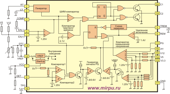
Fig. 2 Functional diagram of the FSP3528 PWM controller
The FSP3528 chip is available in a 20-pin DIP package (Fig. 1). The purpose of the microcircuit contacts is described in Table 1, and Fig. 2 shows it functional diagram. Table 1 shows for each pin of the microcircuit the voltage that should be on the contact when the microcircuit is turned on in a typical manner. A typical application of the FSP3528 chip is its use as part of a power supply control submodule personal computer. This submodule will be discussed in the same article, but a little lower.
Table 1. Pin assignments of the FSP3528 PWM controller
|
№ |
Signal |
I/O |
Description |
|
Entrance |
Supply voltage +5V. |
||
|
COMP |
Exit |
Error amplifier output. Inside the chip, the pin is connected to the non-inverting input of the PWM comparator. A voltage is generated at this pin, which is the difference between the input voltages of the error amplifier E/A+ and E/A - (pin. 3 and pin. 4). During normal operation of the microcircuit, a voltage of about 2.4V is present at the contact. |
|
|
E/A- |
Entrance |
Inverting input of error amplifier. Inside the chip, this input is biased by 1.25V. A reference voltage of 1.25V is formed internal source. During normal operation of the microcircuit, a voltage of 1.23V should be present at the contact. |
|
|
E/A+ |
Entrance |
Non-inverting error amplifier input. This input can be used to monitor the output voltages of the power supply, i.e. this contact can be considered a signal input feedback. In real circuits, a feedback signal is supplied to this contact, obtained by summing all the output voltages of the power supply (+3.3 V /+5 V /+12 V ). During normal operation of the microcircuit, a voltage of 1.24V should be present at the contact. |
|
|
TREM |
Signal delay control contact ON/OFF (control signal for turning on the power supply). A timing capacitor is connected to this pin. If the capacitor has a capacity of 0.1 µF, then the turn-on delay ( Ton ) is about 8 ms (during this time the capacitor is charged to a level of 1.8V), and the turn-off delay ( Toff ) is about 24 ms (during this time, the voltage on the capacitor when it is discharged decreases to 0.6V). During normal operation of the microcircuit, a voltage of about +5V should be present at this contact. |
||
|
Entrance |
Power supply on/off signal input. In the specification for power supply connectors ATX this signal is designated as PS - ON. REM signal is a signal TTL and is compared by an internal comparator with a reference level of 1.4V. If the signal R.E.M. becomes below 1.4V, the PWM chip starts up and the power supply starts working. If the signal R.E.M. installed in high level(more than 1.4V), then the microcircuit is turned off, and accordingly the power supply is turned off. The voltage at this pin can reach a maximum value of 5.25 V, although the typical value is 4.6 V. During operation, a voltage of about 0.2V should be observed at this contact. |
||
|
Frequency setting resistor of the internal oscillator. During operation, a voltage of about 1.25V is present at the contact. |
|||
|
Frequency-setting capacitor of the internal oscillator. During operation, a sawtooth voltage should be observed at the contact. |
|||
|
Entrance |
Overvoltage detector input. The signal from this pin is compared by an internal comparator with an internal reference voltage. This input can be used to control the supply voltage of the microcircuit, to control its reference voltage, as well as to organize any other protection. In typical use, a voltage of approximately 2.5V should be present at this pin during normal operation of the microcircuit. |
||
|
Signal Delay Control Contact PG (Power Good) ). A timing capacitor is connected to this pin. A 2.2 µF capacitor provides a time delay of 250 ms. The reference voltages for this timing capacitor are 1.8V (when charging) and 0.6V (when discharging). Those. when the power supply is turned on, a signal PG is set to a high level at the moment when the voltage on this timing capacitor reaches 1.8V. And when the power supply is turned off, the signal PG is set to a low level at the moment when the capacitor is discharged to a level of 0.6V. The typical voltage at this pin is +5V. |
|||
|
Exit |
Power Good Signal - nutrition is normal. A high signal level means that all output voltages of the power supply correspond to the nominal values, and the power supply is operating normally. A low signal level indicates a faulty power supply. The state of this signal when normal operation The power supply is +5V. |
||
|
VREF |
Exit |
High precision voltage reference with permissible deviation no more than ±2%. A typical value for this reference voltage is 3.5 V. |
|
|
V 3.3 |
Entrance |
Overvoltage protection signal in the +3.3 V channel. Voltage is supplied to the input directly from the +3.3 channel V. |
|
|
Entrance |
Overvoltage protection signal in channel +5 V. Voltage is supplied to the input directly from channel +5 V. |
||
|
V 12 |
Entrance |
Overvoltage protection signal in the +12 V channel. Voltage from the +12 channel is applied to the input V through a resistive divider. As a result of using a divider, a voltage of approximately 4.2V is established on this contact (provided that there are 12 in channel V voltage is +12.5V) |
|
|
Entrance |
Input for additional overvoltage protection signal. This input can be used to organize protection via some other voltage channel. IN practical schemes This contact is used most often for protection against short circuit in channels -5 V and -12 V . In practical circuits, a voltage of about 0.35V is set at this contact. When the voltage rises to 1.25V, the protection is triggered and the microcircuit is blocked. |
||
|
"Earth" |
|||
|
Entrance |
Input for adjusting the “dead” time (the time when the output pulses of the microcircuit are inactive - see Fig. 3). The non-inverting input of the internal dead time comparator is biased by 0.12 V by the internal source. This allows you to set the minimum value of the “measure” time for output pulses. The “dead” time of the output pulses is adjusted by applying to the input DTC constant voltage ranging from 0 to 3.3V. The higher the voltage, the shorter the operating cycle and the longer the “dead” time. This contact is often used to create a “soft” start when the power supply is turned on. In practical circuits, a voltage of approximately 0.18V is set at this pin. |
||
|
Exit |
Collector of the second output transistor. After starting the microcircuit, pulses are formed on this contact, which follow in antiphase to the pulses on contact C1. |
||
|
Exit |
Collector of the first output transistor. After starting the microcircuit, pulses are formed on this contact, which follow in antiphase to the pulses on contact C2. |
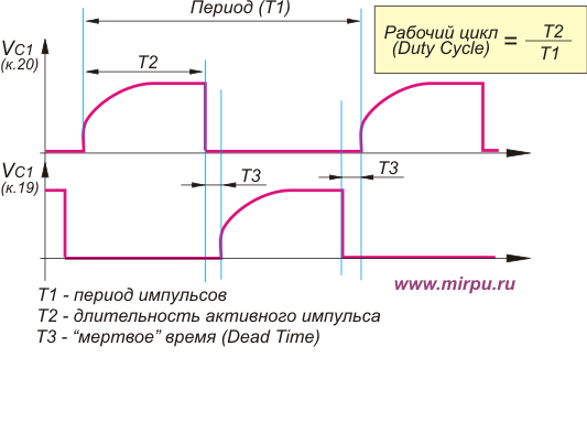 Fig.3 Basic parameters of pulses
The FSP3528 chip is a PWM controller designed specifically to control the push-pull pulse converter of the system power supply of a personal computer. The features of this microcircuit are:
- presence of built-in protection against overvoltage in channels +3.3V/+5V/+12V;
- presence of built-in protection against overload (short circuit) in channels +3.3V/+5V/+12V;
- the presence of a multi-purpose entrance for organizing any protection;
- support for the function of turning on the power supply using the PS_ON input signal;
- the presence of a built-in circuit with hysteresis for generating the PowerGood signal (power supply is normal);
- presence of a built-in precision reference voltage source with a permissible deviation of 2%.
In those power supply models that were listed at the very beginning of the article, the FSP3528 chip is located on the power supply control submodule board. This submodule is located on the secondary side of the power supply and represents printed circuit board, placed vertically, i.e. perpendicular to the main board of the power supply (Fig. 4).
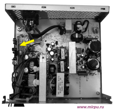
Fig.4 Power supply with FSP3528 module
This submodule contains not only the FSP3528 chip, but also some elements of its “piping” that ensure the functioning of the chip (see Fig. 5).
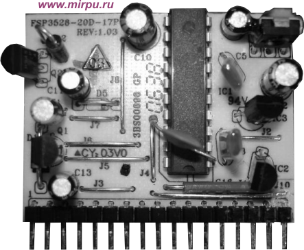
Fig.5 FSP3528 submodule
The control submodule board has double-sided mounting. On the back side of the board there are surface-mounted elements - SMD, which, by the way, give greatest number problems due to not very high quality soldering. The submodule has 17 contacts arranged in one row. The purpose of these contacts is presented in Table 2.
Table 2. Assignment of contacts of the FSPЗ3528-20D-17P submodule
|
№ |
Contact assignment |
|
Output rectangular pulses designed to control power transistors of the power supply |
|
|
Power supply start input signal ( PS_ON) |
|
|
Channel voltage control input +3.3 V |
|
|
Channel voltage control input +5 V |
|
|
Channel voltage control input +12 V |
|
|
Short circuit protection input |
|
|
Not used |
|
|
Power Good Signal Output |
|
|
Voltage regulator cathode AZ431 |
|
|
AZ 431 |
|
|
Regulator reference voltage input AZ 431 |
|
|
Voltage regulator cathode AZ431 |
|
|
Earth |
|
|
Not used |
|
|
Supply voltage VCC |
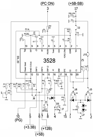
On the control submodule board, in addition to the FSP3528 chip, there are two more controlled stabilizers AZ431(analogous to TL431) which are in no way connected with the FSP3528 PWM controller itself, and are designed to control circuits located on the main board of the power supply.
As an example of the practical implementation of the FSP3528 chip, Fig. 6 shows a diagram of the FSP3528-20D-17P submodule. This control submodule is used in FSP ATX-400PNF power supplies. It is worth noting that instead of a diode D5, a jumper is installed on the board. This sometimes confuses individual specialists who are trying to install a diode in the circuit. Installing a diode instead of a jumper does not change the functionality of the circuit - it should function both with a diode and without a diode. However, installing a diode D5 may reduce the sensitivity of the short circuit protection circuit.

Fig.6 Diagram of the FSP3528-20D-17P submodule
Such submodules are, in fact, the only example application of the FSP3528 microcircuit, therefore a malfunction of the submodule elements is often mistaken for a malfunction of the microcircuit itself. In addition, it often happens that specialists are unable to identify the cause of the malfunction, as a result of which the microcircuit is assumed to be faulty, and the power supply is put aside in the “far corner” or even written off.
In fact, failure of a microcircuit is quite rare. Submodule elements are much more susceptible to failures, and, first of all, semiconductor elements (diodes and transistors).
Today, the main malfunctions of the submodule can be considered:
- failure of transistors Q1 and Q2;
- failure of capacitor C1, which may be accompanied by its “swelling”;
- failure of diodes D3 and D4 (simultaneously or separately).
Failure of the remaining elements is unlikely, however, in any case, if a malfunction of the submodule is suspected, it is necessary to first check the soldering of the SMD components on the printed circuit board side.
Chip diagnostics
Diagnostics of the FSP3528 controller is no different from diagnostics of all other modern PWM controllers for system power supplies, which we have already talked about more than once on the pages of our magazine. But still, once again, in general outline, we’ll tell you how you can verify that the submodule is working properly.
To check, it is necessary to disconnect the power supply with the submodule being diagnosed from the network, and apply all the necessary voltages to its outputs ( +5V, +3.3V, +12V, -5V, -12V, +5V_SB). This can be done using jumpers from another, working, system power supply. Depending on the power supply circuit, you may also need to supply a separate supply voltage +5V on pin 1 of the submodule. This can be done using a jumper between pin 1 of the submodule and the line +5V.
At the same time, on contact C.T.(cont. 8) a sawtooth voltage should appear, and on the contact VREF(pin 12) should appear constant pressure +3.5V.
Next, you need to short-circuit the signal to ground PS-ON. This is done by shorting to ground either the contact of the output connector of the power supply (usually the green wire) or pin 3 of the submodule itself. In this case, rectangular pulses should appear at the output of the submodule (pin 1 and pin 2) and at the output of the FSP3528 microcircuit (pin 19 and pin 20), following in antiphase.
The absence of pulses indicates a malfunction of the submodule or microcircuit.
I would like to note that when using such diagnostic methods, it is necessary to carefully analyze the circuitry of the power supply, since the testing methodology may change slightly, depending on the configuration of the feedback circuits and protection circuits. emergency modes operation of the power supply.
- GTX 1060 Gigabyte Windforce for pennies at XPERT.RU. "> GTX 1060 Gigabyte Windforce for pennies in XPERT.RU.
- GTX 1070 in XPERT.RU - the coolest non-refs for the most low prices
- Lots of GTX 1060 from 17 t.r. in Citylink. We must take it
You can mark fragments of text that interest you,
which will be available via a unique link in address bar browser.
ATX power supply: conversion to a low-frequency amplifier (part 2)
serj 10/22/2011 00:00 Page: 3 of 3| | print version | | archive
- Page 1: Modernization of a switching power supply, problem statement, FSP ATX-300GTF, removal of excess, choosing a method for obtaining increased output voltage, rewinding the transformer, multiplier
- Page 2: Additional transformer, selection and calculation of transformer, rectifier diodes, power supply transformer, inductor
- Page 3: Refinement of the power supply controller circuit, high-frequency interference, observations and conclusions, conclusion
Refinement of the power supply controller circuit
The computer power supply provides many output voltages and must control their presence within specified limits. If the voltage is excessively low or high, the protection should operate and turn off the power supply. The power supply in question does not have such a “menagerie” (it is different) and an attempt to turn it on will lead to an immediate shutdown - the circuit does not have voltages of +5 V and 3.3 V. In fact, they could have been saved, but this would have reduced the space that is already lacks. Well, you'll have to trick the controller and simulate the missing voltages.
In the FSP ATX-300GTF power supply, the control chip is FSP3528. There is not much documentation for it, rather it is completely absent. In terms of pin assignments and control signals, a close (but not complete!) analogue can be called KA3511. As a difference, one immediately notices the different division coefficient of the OVP12 signal, which is where they were going to “climb”. We'll have to look alternative options and the forum of the site rom.by can help with this, from which an approximate trace of the controller on the FSP3528 chip was pulled:
During modification, the power part remains unchanged, but the feedback and protection against over/undershoot need to be adjusted. Let's start with the latter, usually the test unit in the microcircuit is organized as follows (taken from the description of the KA3511 microcircuit):
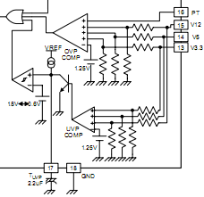
If any output voltage is above the threshold, then the OVP comparator is triggered and the power supply is turned off. When the voltage is too low, the output of the comparator UVP is set to 0, which turns off the transistor and allows the external capacitor Tuvp (via pin 17) to charge. When the capacitor is charged to a voltage of 1.8 V, the output level will be high, which will block the PWM signal and lead to the power supply turning off.
Refinement can be done in two ways - or create standard voltages of 12 V, 5 V and 3.3 V using resistive dividers. Or the second option is to not care about all this unnecessary action and just apply 0 volts to the inputs V12, V5 and V3.3. In this case, the UVP protection will work, but it is blocked by shorting pin 17 to ground - the protection circuit will wait for the shutdown signal “for a very long time.” This solution is good because the output voltage can be anything, even adjustable (adjustable), and the voltage control will not get under your feet. However, if you need control over excess, one or two voltages can be applied to the OVP circuit.
Well, we’ve studied the hardware, we can move on to the FSP3528. And a gift immediately follows - this controller does not have a UVP node and there is no need to do anything with the control inputs, you just need to disconnect them from the rest of the circuit (or short them to ground).
The next step is to rebuild the stabilization chain. Judging by the FSP ATX-300GTF circuit, the controller stabilizes the output voltage at three voltages: 12, 5 and 3.3. I partly understand how 12 V and 5 V were included in this list, but what does 3.3 have to do with it? The meaning escapes. However, this is “their business”; in the modified power supply, the feedback circuit will be redone and all these “excesses” will be removed.
In the first version, feedback was taken from the “+40 V” and “+12 V” outputs through two identical 10 kOhm resistors to a variable resistor. An additional 430 Ohm resistor was installed in the circuit between this point and ground. For reference, Vref = 1.25 V. The output voltage was regulated within +11...+16 V (at the “+12 V” output), the other outputs were changed proportionally.
The modified power supply showed the following results:
| Load current channels, A | Voltage output +12 V, V | Voltage output -12 V, V | Voltage output +40 V, V | Voltage output -40 V, V |
| Idling | 11.60 | -11.66 | 40.90 | -40.88 |
| "+40 V" 1 A | 12.48 | -12.56 | 40.01 | -44.79 |
| "+40 V" 2 A | 12.58 | -12.75 | 39.82 | -46.17 |
| "-40 V" 1 A | 11.50 | -11.50 | 40.93 | -36.88 |
| "-40 V" 2 A | 11.36 | -11.22 | 41.11 | -35.40 |
| "+12 V" 1 A | 11.11 | -11.57 | 41.45 | -41.50 |
| "+12 V" 2 A | 10.92 | -11.58 | 41.62 | -42.09 |
| "-12 V" 1 A | 11.35 | -10.60 | 41.19 | -41.37 |
| "-12 V" 2 A | 11.25 | -10.16 | 41.23 | -41.30 |
| "+40 V" 4 A | 13.09 | -13.24 | 39.47 | -46.71 |
| "-40 V" 4 A | 11.15 | -10.71 | 41.41 | -32.23 |
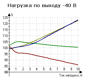
It is quite difficult to represent numerical data in the form quality characteristics, let's try to present the results graphically. If you simply transfer the obtained figures to the graphs, then the positive and negative voltages will “diverge” in different directions, and qualitative comparison it won't work. Let's try differently, recalculate all values to 100%, and for negative values we take the modulus - as a result, all four graphs will run side by side, which is what is required.
Load characteristics were measured only up to four amperes, further increase current was meaningless - the “-40 V” output went beyond the “-25%” threshold:
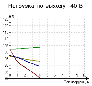
Graph colors:
- Dark red, +40 V.
- Dark green, -40 V.
- Gray, +12 V.
- Blue, -12 V.
Hmmm. The disadvantages of stabilizing only positive voltages are quite clearly visible - the system practically does not “see” the increase in consumption on negative outputs, as a result of which their voltage is greatly reduced. Look at the last two lines - the “+40 V” channel is maintained at about 40 volts, while the “-40 V” does something unintelligible. We will have to introduce negative outputs into the stabilization circuit. However, I don’t need the “+/-12 V” channel, so it’s enough to add only “-40 V”.
In addition to the reduced stability of negative voltages, there is another problem - the level of ripple with the network frequency. With ripple and conversion noise, everything is simple - a larger capacitor, and then another LC filter and the problem goes away. But low-frequency pulsations arise due to ineffective feedback. Why? Instability with the network frequency affects all outputs, which means they must also be present at the positive outputs, covered by feedback, which can eliminate everything. Alas, capacitors of appreciable capacity are installed at the outputs and the load current is very low.
As a result, the capacitors are charged at the peaks of low-frequency pulsations and practically do not change their voltage during the pulsation period. This means that the voltage at the unloaded outputs does not contain ripples and the feedback “does not see” any change, and therefore cannot eliminate them. For example, when only the “-12 V” output is loaded with a current of 2 A, not only its voltage (-10.16 V) is greatly reduced, but also the ripple with the mains frequency increases wildly, up to 1.5 volts. If you create a load current sufficient to discharge the storage capacitors of the feedback channels (“+12 V” or “+40 V”), then the “-12 V” output returns to normal, the ripple value is reduced to 50 mV.
So, there are two problems - expand the feedback by adding a “-40 V” output to it, and somehow introduce feedback via an alternating signal for the same “-40 V” output.
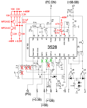
On the diagram, red and green crosses mark elements and routes that should be deleted. In the left top corner added power supply feedback circuit. The “+40 V” output is connected through a 22 kOhm resistor and a 2.2 kOhm + 0.1 μF chain, “+12 V” through a 10 kOhm resistor, and a circuit for inverting the current from the negative “-40 V” output is implemented on the remaining elements. An additional circuit of 47 kOhm and 0.1 µF reduces the ripple level at the -40 V output, which is shown in the upper right part of the figure.
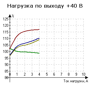
After modification, the power supply showed the following characteristics:
| Load current channels, A | Voltage output +12 V, V | Voltage output -12 V, V | Voltage output +40 V, V | Voltage output -40 V, V |
| Idling | 11.83 | -11.89 | 40.79 | -40.59 |
| "+40 V" 1 A | 12.09 | -12.20 | 38.78 | -42.26 |
| "+40 V" 2 A | 12.18 | -12.34 | 38.54 | -42.26 |
| "+40 V" 4 A | 12.60 | -12.83 | 37.91 | -41.90 |
| "-40 V" 1 A | 12.04 | -12.05 | 41.98 | -38.54 |
| "-40 V" 2 A | 12.24 | -12.15 | 41.84 | -38.21 |
| "-40 V" 4 A | 12.79 | -12.59 | 41.38 | -37.40 |
| "+12 V" 1 A | 11.47 | -11.87 | 41.08 | -40.89 |
| "+12 V" 2 A | 11.26 | -11.80 | 41.22 | -41.20 |
| "-12 V" 1 A | 11.76 | -11.47 | 40.79 | -40.63 |
| "-12 V" 2 A | 11.79 | -10.78 | 40.92 | -40.34 |
| "+40 V" 5 A | 12.95 | -13.11 | 37.44 | -41.53 |
| "-40 V" 5 A | 13.11 | -12.95 | 41.11 | -36.91 |
| “+40 V” 4 A, “-40 V” 1 A | 13.29 | -13.37 | 38.10 | -40.01 |
| "+40 V" 10 A | 14.90 | -15.02 | 35.15 | -39.65 |
| "-40 V" 10 A | 14.71 | -14.77 | 40.19 | -34.37 |
The level of low-frequency pulsations did not exceed 50 mV. What about high frequencies? We should talk about them separately.
The load characteristics are as follows:
The power supply meets the required specifications in all respects, except one - the second channel should be +/-20 V, but it turned out to be +/-12 V. For those purposes, where will he go this power supply, voltage additional channel not significant, so I simply “turned a blind eye” to the violation of this clause. If you need to get a different voltage, more than +/-12 V, then you need to do the same as you did with the main “+/-40 V” channel - use the winding on the second transformer to increase the output voltage level. For example, to get +/-20V you need to follow these steps:
1. A tap should be made on each secondary winding of the additional transformer. In fact, you will have to wind two windings instead of one, with two conductors; there is room on the frame.
2. Obtaining 20 V requires adding 8 V to the existing 12 V. For six turns of the primary winding, additional. The transformer has 11 volts, which means that 8 volts will require 8*6/11=4.3 (four turns).
3. The number of turns of the secondary winding was fifteen, now it is divided into two unequal parts - four and eleven turns.
4. The load current of the “+/-40 V” and “+/-20 V” channels flows through the smaller winding (four turns), so it is worth considering the thickness of the wire used. If the increase in current is not so great, the amplifiers of the LF and MF-HF bands of the amplifier rarely work simultaneously, then you can leave the same wire that is used for the entire winding. If the current level may turn out to be significantly higher in the long term, then it is better to double the number of conductors in this winding.
5. The winding sequence may vary, because the entire winding may not fit on the frame in one layer, but all windings of the same type must have exactly the same number of turns. It is not difficult to fulfill this requirement, you just need to be careful.
There is probably no need to draw a circuit with a modified “+/-20 V” output - if you have figured out the principle of obtaining “+/-40 V”, then exactly the same technique is used here.
High frequency interference
Interference with the converter frequency is the scourge of switching power supplies. Once they arise, they spread throughout all circuits and degrade the performance of devices. They suffer the most from this various types receivers analog signal, especially with a wired connection without electrical insulation. Alas, the “amplifier” has all these “advantages”, so the problem of RF interference is very acute. Let's consider a simplified topology of a half-bridge class pulse converter:
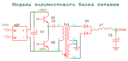
The 220 volt network voltage is rectified by the diode bridge UZ1, smoothed by capacitor C1 and then supplied to the converter. Only drawn from it key transistors, the remaining elements do not affect the level of interference. Transistors Q1 and Q2 are closed alternately, which creates a PWM voltage at the output. Capacitor C2 removes the DC component, and transmits the AC signal without attenuation. From the point of view of the occurrence of interference, it can be mentally “shorted” and, in fact, I drew it in vain, I simply could not suppress the habit of not making unworkable decisions, even in a conditional form.
Voltage on the primary winding of the transformer (pins 6-4) - complex shape with very “sharp” edges with an amplitude of +/-150 volts (+/- half the supply voltage). To be at least somewhat specific, let’s assume that the PWM voltage is generated with a duty cycle of 70% and the output voltage is stabilized at 12 volts. This means that each secondary winding receives a pulse voltage with an amplitude of +/-20 volts.
It is not by chance that I persistently repeat about fronts - the sharper the amplitude of the signal changes, the larger its spectrum. The “small” interwinding capacitance does not conduct the fundamental frequency of the converter well, but the “fronts” are completely different; they produce very high frequency, units of megahertz, and it passes well even through the “small” interwinding capacitance. Therefore, interference is visible at the output voltages not in the form of the conversion frequency (40-80 kHz), but rather “sticks”, a burst of HF oscillations at the moments of the transistor switching fronts.
How can you reduce RF interference? The screen has already been made and its operating efficiency is quite high... but this is not enough. Should I install a filter at the output of the power supply? Good idea, they do this too often effective measure. In this power supply, something similar should definitely be done by passing the output wires of the power supply through a ferrite ring, but these are all means of dealing with the consequences, and not with the disease itself.
There is only one thing left to do - place a small capacitor between the common wires of the primary and secondary sides. Interference is induced between these circuits, which means the capacitor will “suppress” them. The technique is old and has been used for a long time, but it has a drawback that limits its widespread use - the “common” wire of the network part of the circuit is quite “dirty”, with a high level of interference. This is due to the fact that transistors switch high power with low switching time, which produces a high level of RF interference in power circuits.
Installing a capacitor between the “grounds” of the network and output parts reduces the level of noise in the transformer, but adds noise from the power supply circuits of the transistors. Typically, a capacitor of 470 pF - 4.7 nF is used (depending on the value of the active interwinding capacitance) with an operating voltage of at least 3000 volts. I used a regular “Y” capacitor with a capacity of 2.2 nF. The effectiveness of noise suppression can be seen by the leakage current between the “ground” circuits of the network and output parts of the device, for which a 1 kOhm resistor is installed between them and the voltage is measured. Original version located on the left, after adding a capacitor on the right:
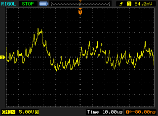
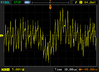
It is clearly visible that the level of interference has decreased several times. But who is interested in any leakage currents? Let's take a look at what changes at the output of the power supply.
On the left is an oscillogram before installing the capacitor, on the right - after:
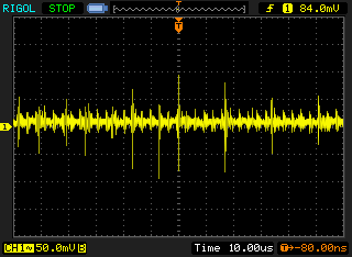
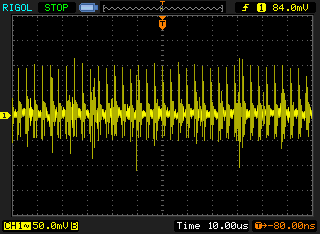
The pictures were taken for a load power of 40 W. And here, too, the differences are visible to the naked eye. Adding a capacitor eliminated the "high frequency noise" that was doing most of the damage. The remaining “sticks” are easily removed by the LC filter on the amplifier board and do not cause problems.
You should not try to obtain a particularly low level of interference in the power supply itself - there is clearly not enough space there for normal routing of the ground circuit, and the compact placement of power elements creates conditions for the propagation of interference through radiation. It’s not for nothing that network power supplies are manufactured as separate devices in a metal case.
Observations and conclusions
After all the modifications and changes, the result was the following power supply:

Its conversion took place without any complications and burnt transistors, which is rare for switching power supplies. The main thing is to be careful not to remove anything unnecessary, especially for the duty source circuits. The efficiency was not specifically measured; at a load of 200 W it is around 86 percent. It’s interesting that before the modification, the power supply showed an efficiency of 76 percent, but the main load was created at the 12 V output. Well, the additional transformer does not significantly impair the performance of the power supply, and this is good news.
As for the power supply itself, with a load of 100 W there are no elements hotter than 40 degrees in it. The power supply has a fan with a thermostat; at low loads, its rotation speed is extremely low and the noise level produced is insignificant. It would be possible to remove it altogether, but the design of the radiators is poorly suited for cooling by natural convection. In addition, the efficiency of the amplifier is by no means 100% and it will also contain a radiator. This means that a fan can be very useful - even with a small amount of airflow, the efficiency of the amplifier’s radiator increases and it can be made smaller.
Refinement of the power supply controller circuit, high-frequency interference, observations and conclusions, conclusion
- GTX 1060 Gigabyte Windforce for pennies at XPERT.RU. "> GTX 1060 Gigabyte Windforce for pennies in XPERT.RU.
- GTX 1070 at XPERT.RU - the coolest unrefs at the lowest prices
- Lots of GTX 1060 from 17 t.r. in Citylink. We must take it
You can mark fragments of text that interest you,
which will be available via a unique link in the browser address bar.
ATX power supply: conversion to a low-frequency amplifier (part 2)
serj 10/22/2011 00:00 Page: 3 of 3| | print version | | archive
- Page 1: Modernization of a switching power supply, problem statement, FSP ATX-300GTF, removal of excess, choosing a method for obtaining increased output voltage, rewinding the transformer, multiplier
- Page 2: Additional transformer, selection and calculation of transformer, rectifier diodes, power supply transformer, inductor
- Page 3: Refinement of the power supply controller circuit, high-frequency interference, observations and conclusions, conclusion
Refinement of the power supply controller circuit
The computer power supply provides many output voltages and must control their presence within specified limits. If the voltage is excessively low or high, the protection should operate and turn off the power supply. The power supply in question does not have such a “menagerie” (it is different) and an attempt to turn it on will lead to an immediate shutdown - the circuit does not have voltages of +5 V and 3.3 V. In fact, they could have been saved, but this would have reduced the space that is already lacks. Well, you'll have to trick the controller and simulate the missing voltages.
In the FSP ATX-300GTF power supply, the control chip is FSP3528. There is not much documentation for it, rather it is completely absent. In terms of pin assignments and control signals, a close (but not complete!) analogue can be called KA3511. As a difference, one immediately notices the different division coefficient of the OVP12 signal, which is where they were going to “climb”. You will have to look for alternative options, and the forum of the site rom.by can help with this, from which an approximate trace of the controller on the FSP3528 chip was pulled:
During modification, the power part remains unchanged, but the feedback and protection against over/undershoot need to be adjusted. Let's start with the latter, usually the test unit in the microcircuit is organized as follows (taken from the description of the KA3511 microcircuit):
If any output voltage is above the threshold, then the OVP comparator is triggered and the power supply is turned off. When the voltage is too low, the output of the comparator UVP is set to 0, which turns off the transistor and allows the external capacitor Tuvp (via pin 17) to charge. When the capacitor is charged to a voltage of 1.8 V, the output level will be high, which will block the PWM signal and lead to the power supply turning off.
Refinement can be done in two ways - or create standard voltages of 12 V, 5 V and 3.3 V using resistive dividers. Or the second option is to not care about all this unnecessary action and just apply 0 volts to the inputs V12, V5 and V3.3. In this case, the UVP protection will work, but it is blocked by shorting pin 17 to ground - the protection circuit will wait for the shutdown signal “for a very long time.” This solution is good because the output voltage can be anything, even adjustable (adjustable), and the voltage control will not get under your feet. However, if you need control over excess, one or two voltages can be applied to the OVP circuit.
Well, we’ve studied the hardware, we can move on to the FSP3528. And a gift immediately follows - this controller does not have a UVP node and there is no need to do anything with the control inputs, you just need to disconnect them from the rest of the circuit (or short them to ground).
The next step is to rebuild the stabilization chain. Judging by the FSP ATX-300GTF circuit, the controller stabilizes the output voltage at three voltages: 12, 5 and 3.3. I partly understand how 12 V and 5 V were included in this list, but what does 3.3 have to do with it? The meaning escapes. However, this is “their business”; in the modified power supply, the feedback circuit will be redone and all these “excesses” will be removed.
In the first version, feedback was taken from the “+40 V” and “+12 V” outputs through two identical 10 kOhm resistors to a variable resistor. An additional 430 Ohm resistor was installed in the circuit between this point and ground. For reference, Vref = 1.25 V. The output voltage was regulated within +11...+16 V (at the “+12 V” output), the other outputs were changed proportionally.
The modified power supply showed the following results:
| Load current channels, A | Voltage output +12 V, V | Voltage output -12 V, V | Voltage output +40 V, V | Voltage output -40 V, V |
| Idling | 11.60 | -11.66 | 40.90 | -40.88 |
| "+40 V" 1 A | 12.48 | -12.56 | 40.01 | -44.79 |
| "+40 V" 2 A | 12.58 | -12.75 | 39.82 | -46.17 |
| "-40 V" 1 A | 11.50 | -11.50 | 40.93 | -36.88 |
| "-40 V" 2 A | 11.36 | -11.22 | 41.11 | -35.40 |
| "+12 V" 1 A | 11.11 | -11.57 | 41.45 | -41.50 |
| "+12 V" 2 A | 10.92 | -11.58 | 41.62 | -42.09 |
| "-12 V" 1 A | 11.35 | -10.60 | 41.19 | -41.37 |
| "-12 V" 2 A | 11.25 | -10.16 | 41.23 | -41.30 |
| "+40 V" 4 A | 13.09 | -13.24 | 39.47 | -46.71 |
| "-40 V" 4 A | 11.15 | -10.71 | 41.41 | -32.23 |
It is quite difficult to present numerical data in the form of qualitative characteristics; let’s try to present the results graphically. If you simply transfer the obtained figures to the graphs, then the positive and negative voltages will “diverge” in different directions, and a qualitative comparison will not be possible. Let's try differently, recalculate all values to 100%, and for negative values we take the modulus - as a result, all four graphs will run side by side, which is what is required.
Load characteristics were measured only up to four amperes; further increase in current was pointless - the “-40 V” output went beyond the “-25%” threshold:
Graph colors:
- Dark red, +40 V.
- Dark green, -40 V.
- Gray, +12 V.
- Blue, -12 V.
Hmmm. The disadvantages of stabilizing only positive voltages are quite clearly visible - the system practically does not “see” the increase in consumption on negative outputs, as a result of which their voltage is greatly reduced. Look at the last two lines - the “+40 V” channel is maintained at about 40 volts, while the “-40 V” does something unintelligible. We will have to introduce negative outputs into the stabilization circuit. However, I don’t need the “+/-12 V” channel, so it’s enough to add only “-40 V”.
In addition to the reduced stability of negative voltages, there is another problem - the level of ripple with the network frequency. With ripple and conversion noise, everything is simple - a larger capacitor, and then another LC filter and the problem goes away. But low-frequency pulsations arise due to ineffective feedback. Why? Instability with the network frequency affects all outputs, which means they must also be present at the positive outputs, covered by feedback, which can eliminate everything. Alas, capacitors of appreciable capacity are installed at the outputs and the load current is very low.
As a result, the capacitors are charged at the peaks of low-frequency pulsations and practically do not change their voltage during the pulsation period. This means that the voltage at the unloaded outputs does not contain ripples and the feedback “does not see” any change, and therefore cannot eliminate them. For example, when only the “-12 V” output is loaded with a current of 2 A, not only its voltage (-10.16 V) is greatly reduced, but also the ripple with the mains frequency increases wildly, up to 1.5 volts. If you create a load current sufficient to discharge the storage capacitors of the feedback channels (“+12 V” or “+40 V”), then the “-12 V” output returns to normal, the ripple value is reduced to 50 mV.
So, there are two problems - expand the feedback by adding a “-40 V” output to it, and somehow introduce feedback via an alternating signal for the same “-40 V” output.
On the diagram, red and green crosses mark elements and routes that should be deleted. A power supply feedback circuit has been added in the upper left corner. The “+40 V” output is connected through a 22 kOhm resistor and a 2.2 kOhm + 0.1 μF chain, “+12 V” through a 10 kOhm resistor, and a circuit for inverting the current from the negative “-40 V” output is implemented on the remaining elements. An additional circuit of 47 kOhm and 0.1 µF reduces the ripple level at the -40 V output, which is shown in the upper right part of the figure.
After modification, the power supply showed the following characteristics:
| Load current channels, A | Voltage output +12 V, V | Voltage output -12 V, V | Voltage output +40 V, V | Voltage output -40 V, V |
| Idling | 11.83 | -11.89 | 40.79 | -40.59 |
| "+40 V" 1 A | 12.09 | -12.20 | 38.78 | -42.26 |
| "+40 V" 2 A | 12.18 | -12.34 | 38.54 | -42.26 |
| "+40 V" 4 A | 12.60 | -12.83 | 37.91 | -41.90 |
| "-40 V" 1 A | 12.04 | -12.05 | 41.98 | -38.54 |
| "-40 V" 2 A | 12.24 | -12.15 | 41.84 | -38.21 |
| "-40 V" 4 A | 12.79 | -12.59 | 41.38 | -37.40 |
| "+12 V" 1 A | 11.47 | -11.87 | 41.08 | -40.89 |
| "+12 V" 2 A | 11.26 | -11.80 | 41.22 | -41.20 |
| "-12 V" 1 A | 11.76 | -11.47 | 40.79 | -40.63 |
| "-12 V" 2 A | 11.79 | -10.78 | 40.92 | -40.34 |
| "+40 V" 5 A | 12.95 | -13.11 | 37.44 | -41.53 |
| "-40 V" 5 A | 13.11 | -12.95 | 41.11 | -36.91 |
| “+40 V” 4 A, “-40 V” 1 A | 13.29 | -13.37 | 38.10 | -40.01 |
| "+40 V" 10 A | 14.90 | -15.02 | 35.15 | -39.65 |
| "-40 V" 10 A | 14.71 | -14.77 | 40.19 | -34.37 |
The level of low-frequency pulsations did not exceed 50 mV. What about high frequencies? We should talk about them separately.
The load characteristics are as follows:
The power supply meets the required specifications in all respects, except one - the second channel should be +/-20 V, but it turned out to be +/-12 V. For the purposes for which this power supply will be used, the voltage of the additional channel is not significant, so there is no violation At this point I simply “closed my eyes.” If you need to get a different voltage, more than +/-12 V, then you need to do the same as you did with the main “+/-40 V” channel - use the winding on the second transformer to increase the output voltage level. For example, to get +/-20V you need to follow these steps:
1. A tap should be made on each secondary winding of the additional transformer. In fact, you will have to wind two windings instead of one, with two conductors; there is room on the frame.
2. Obtaining 20 V requires adding 8 V to the existing 12 V. For six turns of the primary winding, additional. The transformer has 11 volts, which means that 8 volts will require 8*6/11=4.3 (four turns).
3. The number of turns of the secondary winding was fifteen, now it is divided into two unequal parts - four and eleven turns.
4. The load current of the “+/-40 V” and “+/-20 V” channels flows through the smaller winding (four turns), so it is worth considering the thickness of the wire used. If the increase in current is not so great, the amplifiers of the LF and MF-HF bands of the amplifier rarely work simultaneously, then you can leave the same wire that is used for the entire winding. If the current level may turn out to be significantly higher in the long term, then it is better to double the number of conductors in this winding.
5. The winding sequence may vary, because the entire winding may not fit on the frame in one layer, but all windings of the same type must have exactly the same number of turns. It is not difficult to fulfill this requirement, you just need to be careful.
There is probably no need to draw a circuit with a modified “+/-20 V” output - if you have figured out the principle of obtaining “+/-40 V”, then exactly the same technique is used here.
High frequency interference
Interference with the converter frequency is the scourge of switching power supplies. Once they arise, they spread throughout all circuits and degrade the performance of devices. Most of all, various types of analog signal receivers suffer from this, especially those with a wired connection without electrical insulation. Alas, the “amplifier” has all these “advantages”, so the problem of RF interference is very acute. Let's consider a simplified topology of a half-bridge class pulse converter:
The 220 volt network voltage is rectified by the diode bridge UZ1, smoothed by capacitor C1 and then supplied to the converter. Only key transistors are drawn from it; the remaining elements do not affect the noise level. Transistors Q1 and Q2 are closed alternately, which creates a PWM voltage at the output. Capacitor C2 removes the DC component, and transmits the AC signal without attenuation. From the point of view of the occurrence of interference, it can be mentally “shorted” and, in fact, I drew it in vain, I simply could not suppress the habit of not making unworkable decisions, even in a conditional form.
The voltage on the primary winding of the transformer (pins 6-4) is of a complex shape with very “sharp” edges with an amplitude of +/-150 volts (+/- half the supply voltage). To be at least somewhat specific, let’s assume that the PWM voltage is generated with a duty cycle of 70% and the output voltage is stabilized at 12 volts. This means that each secondary winding receives a pulse voltage with an amplitude of +/-20 volts.
It is no coincidence that I persistently repeat about fronts - the sharper the amplitude of the signal changes, the larger its spectrum. The “small” interwinding capacitance does not conduct well the fundamental frequency of the converter, but the “fronts” are completely different, they produce a very high frequency, several megahertz, and it passes well even through the “small” interwinding capacitance. Therefore, interference is visible at the output voltages not in the form of the conversion frequency (40-80 kHz), but rather “sticks”, a burst of RF oscillations at the moments of the transistor switching fronts.
How can you reduce RF interference? The screen has already been made and its operating efficiency is quite high... but this is not enough. Should I install a filter at the output of the power supply? Good idea, this is often done and it is an effective measure. In this power supply, something similar should definitely be done by passing the output wires of the power supply through a ferrite ring, but these are all means of dealing with the consequences, and not with the disease itself.
There is only one thing left to do - place a small capacitor between the common wires of the primary and secondary sides. Interference is induced between these circuits, which means the capacitor will “suppress” them. The technique is old and has been used for a long time, but it has a drawback that limits its widespread use - the “common” wire of the network part of the circuit is quite “dirty”, with a high level of interference. This is due to the fact that transistors switch high power with low switching time, which produces a high level of RF interference in power circuits.
Installing a capacitor between the “grounds” of the network and output parts reduces the level of noise in the transformer, but adds noise from the power supply circuits of the transistors. Typically, a capacitor of 470 pF - 4.7 nF is used (depending on the value of the active interwinding capacitance) with an operating voltage of at least 3000 volts. I used a regular "Y" capacitor with a capacity of 2.2 nF. The effectiveness of noise suppression can be seen by the leakage current between the “ground” circuits of the network and output parts of the device, for which a 1 kOhm resistor is installed between them and the voltage is measured. The original version is located on the left, after adding a capacitor on the right:
It is clearly visible that the level of interference has decreased several times. But who is interested in any leakage currents? Let's take a look at what changes at the output of the power supply.
On the left is an oscillogram before installing the capacitor, on the right - after:
The pictures were taken for a load power of 40 W. And here, too, the differences are visible to the naked eye. Adding a capacitor eliminated the "high frequency noise" that was doing most of the damage. The remaining “sticks” are easily removed by the LC filter on the amplifier board and do not cause problems.
You should not try to obtain a particularly low level of interference in the power supply itself - there is clearly not enough space there for normal routing of the ground circuit, and the compact placement of power elements creates conditions for the propagation of interference through radiation. It’s not for nothing that network power supplies are manufactured as separate devices in a metal case.
Observations and conclusions
After all the modifications and changes, the result was the following power supply:
Its conversion took place without any complications and burnt transistors, which is rare for switching power supplies. The main thing is to be careful not to remove anything unnecessary, especially for the duty source circuits. The efficiency was not specifically measured; at a load of 200 W it is around 86 percent. It’s interesting that before the modification, the power supply showed an efficiency of 76 percent, but the main load was created at the 12 V output. Well, the additional transformer does not significantly impair the performance of the power supply, and this is good news.
As for the power supply itself, with a load of 100 W there are no elements hotter than 40 degrees in it. The power supply has a fan with a thermostat; at low loads, its rotation speed is extremely low and the noise level produced is insignificant. It would be possible to remove it altogether, but the design of the radiators is poorly suited for cooling by natural convection. In addition, the efficiency of the amplifier is by no means 100% and it will also contain a radiator. This means that a fan can be very useful - even with a small amount of airflow, the efficiency of the amplifier’s radiator increases and it can be made smaller.
Refinement of the power supply controller circuit, high-frequency interference, observations and conclusions, conclusion