A linear stabilizer is a voltage divider, the input of which is supplied with an input (unstable) voltage, and the output (stabilized) voltage is removed from the lower arm of the divider. Stabilization carried out by changes in the resistance of one of the arms divider: the resistance is constantly maintained so that the voltage at the output of the stabilizer is within the established limits. With a large ratio of input/output voltages, the linear stabilizer has low efficiency, since most of the power Pdis = (Uin - Uout) * It is dissipated as heat on the control element. Therefore, the control element must be able to dissipate sufficient power, that is, it must be installed on a radiator of the required area. The advantage of a linear stabilizer is its simplicity, lack of interference and a small number of parts used.
Depending on the location of an element with variable resistance linear stabilizers are divided into two types:
− consistent: the control element is connected in series with the load.
− parallel: the regulating element is connected in parallel with the load.
Depending on the stabilization method:
− parametric: in such a stabilizer, a section of the current-voltage characteristic (volt-ampere characteristic) of the device, which has a large steepness, is used.
− compensatory: has feedback. In it, the voltage at the output of the stabilizer is compared with the reference one, and a control signal for the regulating element is formed from the difference between them. They are quite versatile and can be manufactured in the form of integrated circuits for voltage stabilizers.
Linear voltage stabilizer (LCH) chips include, in addition to power regulators, a more or less complex low-power control circuit. Fundamental difficulty the creation of integrated stabilizers is that power transistors dissipate significant power, calling local heating of the crystal with a significant temperature gradient. This dramatically deteriorates the stability of the control circuit parameters, which includes a reference voltage source, a differential error amplifier, overcurrent protection circuits, and short circuit load, from overheating of the crystal and other emergency or abnormal modes.
Monolithic linear integral stabilizer voltage was first developed by R. Widlar in 1967. This microcircuit (pA723) contains a control transistor connected in series between the unstabilized voltage source and the load, an error amplifier and a temperature-compensated reference voltage source. The scheme turned out to be so successful that in the early 70s its production reached 2 million units per month! By mass numbers application of LCH stand on second place after operational amplifiers.
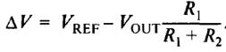
A simplified diagram of a linear voltage stabilizer is shown in Fig. 1.
Rice. 1. Basic circuit of a linear voltage regulator
The circuit consists of an operational amplifier in a non-inverting connection with negative voltage feedback, a reference voltage source V REF and regulating transistor VT 1 connected in series with the load.
Output voltage V OUT controlled by negative circuit feedback, made on a resistive divider R 1 R 2.
The op-amp plays the role of an error amplifier, which here is the difference between the reference voltage V REF specified by the reference voltage source (VR), and the output voltage of the divider R 1 R 2
The scheme works as follows. Let, for one reason or another (for example, due to a decrease in load resistance or unregulated input voltage), the output voltage of the stabilizer V OUT decreased. In this case, an error will appear at the op-amp input V > 0. The output voltage of the amplifier will increase, which will lead to an increase in the base current, and, consequently, the emitter current of the control transistor to a value at which the output voltage will increase almost to the original level.
In the case of an ideal op-amp, the steady-state error value, which coincides with the op-amp's differential input voltage, is close to zero. It follows that
The operational amplifier is powered from an input unregulated unipolar voltage, in this case positive (with a regulating transistor p-n-p -type all voltages in the circuit must be negative). This imposes restrictions on the permissible range of input and output signals, which under these conditions should only be positive
For power supply circuits, such a limitation does not matter, so you can refuse to use a voltage of a different polarity to power the op-amp. Another advantage of such a scheme is that voltage power supply of the operational amplifier can be double , without fear of exceeding its maximum permissible parameters. Thus, standard op-amps can be used in regulator circuits with input voltages up to 30 V. Although the op-amp is powered by an unregulated input voltage V IN , due to deep negative feedback, the influence of this factor on the stability of the output voltage is small.
To power electronic equipment, voltage ripple not exceeding a fraction of a percent is allowed, but at the output of rectifiers the ripple is much greater. To reduce them, smoothing filters are used, which should reduce (suppress) the variable components as much as possible and pass the direct component of the rectified voltage with as little loss as possible.
Rice. 2.30.
A – RC filter; b – a graph explaining the operation of the filter: V - LC filter; G – U-shaped RC filter
The simplest filter is a capacitor connected at the output of the rectifier IN parallel to the load (Fig. 2.30, A), which stores energy by charging when the rectifier voltage increases, and releases it by discharging into the load resistance when it decreases. In Fig. 2.30, b shows the voltage waveform across the capacitor U c (and therefore on a parallel connected R n ) with a full-wave rectifier.
To further reduce ripple, L-shaped LC filters are used (Fig. 2.30, V). Inductive reactance tends to be made much larger R n so that the alternating components of the rectified voltage with ripple frequencies from the main one and higher would be “delayed” by the filter in the form of a voltage drop across X L without reaching the load. Capacitance is significantly less than R H, so that the alternating components of the rectified current are closed through X with, bypassing R,. In this case, the constant current component, for which , does not create a voltage drop across L f and is not closed through Sf, entering the load entirely.
The disadvantage of LC filters is the bulkiness and difficulty of manufacturing microelectronic inductors. Therefore, in integrated circuits at load currents of several milliamps, U-shaped RC filters are used (Fig. 2.30, G), despite their slightly worse smoothing properties and lower efficiency.
Linear voltage stabilizers
Voltage stabilizer is a device that automatically maintains the voltage on the load when such destabilizing factors as the voltage of the primary source, load resistance, and ambient temperature change within certain limits.
There are two types of stabilizers - parametric and compensation.
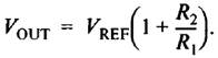
Parametric stabilizer uses elements in which the voltage remains unchanged when the current flowing through them changes. Such elements are zener diodes, in which, when the current changes within a very wide range, the voltage drop changes by fractions of a percent (see paragraph 1.2). Parametric stabilizers are used, as a rule, as sources of reference (reference) voltage in powerful compensation stabilizers (Fig. 2.31).
Rice. 2.31. The structure of a compensation voltage stabilizer (a), its simplest implementation(b) and a graph explaining the choice of operating point(V)
Principle of operation compensation stabilizer is based on comparing the actual load voltage with the reference voltage and increasing or decreasing the output voltage deviation depending on this deviation. The reference voltage is formed by a reference voltage source (VS). In the comparing element (CE), the load voltage is compared with the reference voltage and a mismatch control signal is generated. This signal is amplified by an amplifier (U) and fed to a regulating element (RE), which provides such a change in the output voltage that brings the actual load voltage closer to the reference value.
The main parameter of the stabilizer is stabilization coefficient – the ratio of the relative change in voltage at the input to the relative change in voltage at the output:
In the simplest compensation stabilizer, the reference voltage is the voltage U st zener diode VD, and the comparing element, amplifier and at the same time regulating element is a transistor (see Fig. 2.31, b).
Output voltage (as can be seen from the “+” and “-” signs on the diagram) Uout = U st – UEB. The current through the resistor RB is formed by adding two currents: the zener diode current I st and current base I B. The operating mode of the transistor is selected so that the initial operating point R was located in the middle of the linear section of it input characteristics(see Fig. 2.31, V). Voltage U In this case, the EB is 0.-0.3 V. Since the zener diode voltage is usually about 8 V, then U out ≈ U CT.
Let's assume that for some reason the load voltage has decreased. This will lead to an increase in the voltage drop UEB =U st – U out, which, in turn, will increase the degree of opening of the transistor. As a result, the voltage drop across the transistor U KE will decrease, which means the load voltage will increase U out= U BX – U ΚE, and eventually the voltage at the load will be restored. A similar recovery of the output voltage will occur when it increases. Only in this case will there be a decrease in the degree of opening of the transistor and a corresponding increase in the voltage dropped across it U ke.
The transistor is connected according to the emitter follower circuit, the input voltage of which is U CT. Because I B << I n, the circuit allows you to deliver significant power to the load. The stabilization coefficient of such a scheme is TO st = 150–300. In the considered circuit, the mismatch signal is generated on the control transistor itself. A high degree of stabilization is provided by circuits in which a pre-amplified mismatch signal is supplied to the base of the control transistor.
In the voltage stabilizers considered, the regulating transistor is always open, and self-regulation is carried out by changing the degree of its opening, i.e. linear. Therefore, such stabilizers are called linear.
Switching voltage stabilizers
Unlike the previously discussed linear stabilizers, in pulse voltage stabilizers the transistor through which current flows to the load periodically opens and closes, i.e. works in key mode. Moreover, regulation is carried out by changing the pause, during which the load current flows through the key transistor from a constant input voltage source. Thus, the transistor operates not in a linear mode, but in a pulsed mode: it is either completely open or completely closed. In such stabilizers, the average voltage across the load Uout = U BX t / T, where T - pulse repetition period; t – duration of the key's closed state.
Switching stabilizers provide higher efficiency, since in a fully open state very little voltage drops across the transistor, and therefore the power dissipated by the transistor is much less than the power dissipated in linear stabilizers.
Since regulation is carried out by changing the pulse width t, This operating principle is called pulse width modulation (PWM). Pulse stabilizers (Fig. 2.32), like linear ones, are compensatory. Error signal U p, formed by the comparing element of the SE and amplified by the amplifier (A), is converted into pulses following with the same frequency, the duration of which t on changes under the influence of the error signal. These pulses open and close the key transistor V.T. which together with the diode V.D. and an LC filter forms a pulse regulating element.
![]()
Rice. 2.32. Switching voltage stabilizer (a ) and the processes occurring in it(b)
While the sawtooth voltage U P < U p (section t0 – t1 in Fig. 2.32, b), transistor is locked. For a time t 1 – t 3 when U P >U p, the transistor is open and voltage t/BX is applied to the inductor. UBX driven diode V.D. is locked, and the current through the inductor i dr increases, storing energy in inductance. Until the inductor current reaches the value direct current loads I n (section t 1 – t 2), capacitor WITH discharges to the load and the voltage on it U c decreases. From the moment of time ί2> when i etc > I n the capacitor will begin to recharge by the current difference i dr – I n. At the moment t3 of turning off the transistor, the self-inductive emf of the inductor opens the diode and the inductor current, closing through the diode, flows through the load and until t 4 continues to charge the capacitor, giving it the energy stored by the inductor. In the t4 – t5 section, the inductor current is less than the load current and the load is fed by the capacitor discharge current. Since t 5 the process is repeated.
Let the output voltage become less than the set value and the mismatch voltage U p will decrease by -ΔUρ. Then the moment in time when the sawtooth voltage generated by the GPN becomes equal to the voltage U p will come earlier, and the open state of the transistor ton, generated by PWM, will increase. This will cause the UBbIX output voltage to increase and restore the set value. If the output voltage increases, the error voltage will also increase by +Δ U p. This will lead to the fact that the moment of opening of the transistor, generated by PWM, will come later, and the time of the open state of the transistor ton will decrease. As a result, the output voltage will decrease and its set value will be restored.
Voltage stabilization in modern electronic devices Very important element. Digital circuits require stable and reliable power.
The most simple circuit voltage stabilization that we can find in practice is a system based on a zener diode. The basic operating mode of a zener diode is shown in the following figure:
This system uses the zener diode effect that occurs during breakdown p-n junction at reverse bias. This causes current to flow and any excess voltage is absorbed across the ballast resistor. The amount of voltage drop is determined by the amount of current flowing through it.
Therefore, a fixed current through the zener diode fixes the voltage drop across the resistor and thereby stabilizes the output voltage. Zener diodes are manufactured for various voltages in the range from 1.5V to 200V.
But, often in practice, specialized microcircuits are used to stabilize voltage, which can be divided into two groups:
- with voltage adjustment
- positive polarity
- negative polarity - without voltage adjustment
- positive polarity
- negative polarity
Integrated voltage stabilizers have three main characteristics:
- output voltage
- maximum current
- minimum input voltage
At the input of the voltage stabilizer, it is necessary to apply a higher voltage than what should be at the output.
In the most common stabilizers, the difference between the input and output voltage is about 2V. But there are also LDO stabilizers, in which this difference is much lower. This voltage is often referred to as VDO
Among the popular non-adjustable stabilizers are:
78xx– the most famous of all positive voltage stabilizers. Available in various voltage versions: 5, 6, 8, 9, 10, 12, 15, 18, 24 volts, VDO = 2V.
79xx– the most popular of all negative voltage stabilizers. Produced in voltage versions: 5, 6, 8, 9, 10, 12, 15, 18, 24 volts, VDO = 2V.
LM2940x– LDO positive voltage stabilizer. For voltage: 5, 8, 9, 10, 12, 15 volts, VDO = 0.5V.
Among the adjustable voltage stabilizers, the most famous are:
– output voltage range from 1.25 to 37 volts, VDO = 3V.
LM337– output voltage range from -1.25 – 37 volts, VDO = 5V.
Modern voltage stabilizers have various kinds thermal and current protection, which ensures safe operation and reduces the chances of circuits burning out.
In addition to linear stabilizers, there is also a group of switching stabilizers. They differ, of course, in that they have greater efficiency (less energy is spent on heat losses). Interesting feature is that they allow you to raise and lower voltages, which is very useful when powering microcircuits from a battery.
The linear stabilizer is the original form of stabilizing power supplies. To lower the input voltage level to a stabilized output voltage, it uses variable conductivity of the active electronic element. In this case, the linear stabilizer loses a lot of energy in the form of heat and therefore heats up.
Linear power supplies occupy a significant niche in applications where the low efficiency of such sources does not play a special role. These applications include stationary ground equipment, for which forced air cooling is not a problem. This also includes instruments in which the meter is so sensitive to electrical noise that it requires an electrically “quiet” power source. Such devices include audio and video amplifiers, radios, etc. Linear stabilizers are also popular as local, on-board stabilizers. In this case, the board only requires a few watts, so a few more watts lost in heat can be counteracted with a simple heatsink. If dielectric isolation is required from the AC input source, it is provided by an AC transformer or main power supply system.
In general, linear regulators are especially useful for power supply applications requiring no more than 10 W of output power. At output power greater than 10 W, the required heat sink becomes so bulky and expensive that it becomes more attractive pulsed sources nutrition.
Operating principle of a linear stabilizer
All power supplies - be they linear or more complex switching ones - work the same way basic principle. All power sources are based on closed loop negative feedback. The only purpose of this circuit is to keep the output voltage constant.
Linear stabilizers are only step-down. This means that the input voltage of the source must be higher than the required output voltage. There are two types of linear stabilizers: parallel (shunt) and serial (series-pass). Parallel stabilizer (stabilizer with parallel connection regulating element) is a voltage stabilizer connected in parallel with the load. The unregulated current source is connected to a higher voltage source, the parallel regulator takes the output current to maintain DC voltage on the load, taking into account the variable input voltage and load current. A common example of such a stabilizer is a zener diode stabilizer. A series linear regulator is more efficient than a parallel regulator and uses an active semiconductor between the input source and the load as a series-connected regulating element.
A series-connected feedthrough element operates in linear mode. This means that it was not designed to operate in fully ON or fully OFF mode, but rather operates in a "partially ON" mode. The negative feedback loop determines the amount of conductivity the pass element must accept to provide the required output voltage level.
The heart of the negative feedback loop is a high-gain operational amplifier called an error voltage amplifier. Its purpose is to constantly compare the difference between a highly stable reference voltage and the output voltage. If this difference is at least millivolts, then the electrical conductivity of the passage element is adjusted. A stable reference voltage is supplied to the non-inverting input of the op amp and is typically lower than the output voltage. The output voltage is divided to the reference level and fed to the inverse input of the op-amp. Thus, at rated output voltage, the center point of the output voltage divider is identical to the reference voltage.
The bias amplifier gain provides a voltage corresponding to the greatly increased difference between the reference and output voltages (error voltage). The error voltage directly controls the conductivity of the pass element, thereby maintaining the rated output voltage. As the load increases, the output voltage drops, which leads to an increase in the output power of the amplifier, which provides more current to the load. Likewise, as the load decreases, the output voltage will increase, to which the error amplifier will respond by decreasing the current through the pass element to the load.
The speed with which the error amplifier responds to any changes in output, and how accurately the required output voltage level is maintained, depends on the compensation of the error amplifier feedback loop. Feedback compensation is controlled by placing elements inside the voltage divider and between the negative input and output of the error amplifier. Its design dictates how much DC gain is performed, which in turn determines the accuracy of the output voltage. It also determines the amount of gain at increased frequency and bandwidth, which in turn determines the time taken to respond to changes in output load, or the duration of transients.
As you can see, the operating principle of a linear stabilizer is very simple. Exactly the same circuit is present in all stabilizers, including more complex switching stabilizers. The voltage feedback loop performs the final function of the power supply: maintaining the output voltage level.
Voltage regulator- converter electrical energy, which makes it possible to obtain an output voltage that is within specified limits with significantly larger fluctuations in the input voltage and load resistance.
Based on the type of output voltage, stabilizers are divided into DC and AC stabilizers. As a rule, the type of power supply (constant or alternating current) is the same as the output voltage, although exceptions are possible.